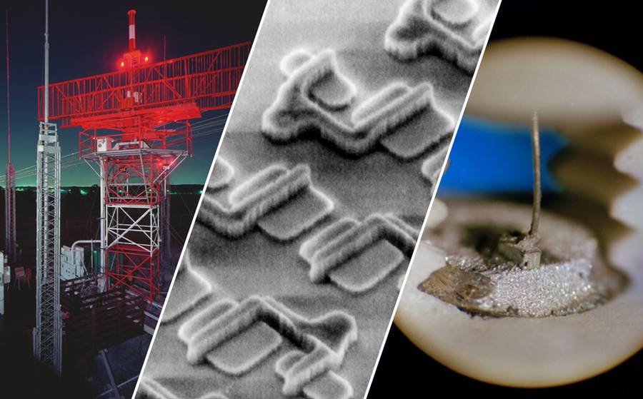
The Institute of Electrical and Electronics Engineers (IEEE) designated three historical MIT Lincoln Laboratory technologies as IEEE Milestones. The technologies are the Mode S air traffic control (ATC) radar beacon system, 193-nanometer (nm) photolithography, and the semiconductor laser. The latter recognition is shared by Lincoln Laboratory, General Electric, and IBM.
As the world's largest technical professional organization, the IEEE's mission is to "advance technology for the benefit of humanity." The Milestone program commemorates innovations developed at least 25 years ago that have done just that.
All three technologies are integral to everyday life. Anyone who has flown on commercial aircraft has benefited from Mode S, the system that air traffic controllers use to track planes. The integrated circuits that power modern computing and communication devices were manufactured using 193 nm photolithography. Perhaps most ubiquitous of all is the semiconductor laser — a micrometer-sized light-emitting device that has made possible high-speed internet, among many other technologies underpinning today's information society.
"MIT Lincoln Laboratory has been a leader in fostering innovations that were previously only considered possible in science fiction. The three IEEE Milestones presented are a testament to those accomplishments and a celebration of the diversity of ingenuity and teamwork that created these game-changing technologies," says Karen Panetta, vice chair of IEEE Boston Section, which presented the awards to Lincoln Laboratory at a ceremony on Feb. 2.
Lincoln Laboratory holds three previous IEEE Milestones for pioneering the use of packet networks for speech communications, for developing the nation's first air defense system, and for creating the Whirlwind high-speed digital computer in collaboration with MIT campus.
Tracking aircraft globally
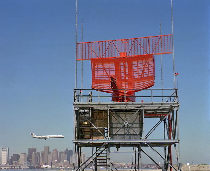
The Mode S ATC radar beacon system was developed to address the challenges posed to the existing ATC beacon-radar system used in the late 1960s. Commercial air traffic was growing quickly, causing interference between beacon replies and interrogations from ATC ground radars. This interference threatened to disrupt aircraft surveillance in high-density airspace.
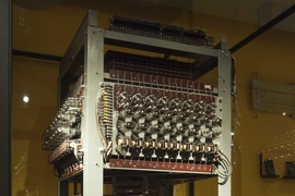
Under Federal Aviation Administration (FAA) sponsorship, Lincoln Laboratory led the technology developments necessary to address this safety issue. The advanced communication architecture of Mode S allowed radars to select a specific aircraft to interrogate. To selectively communicate, the system design included improved aircraft transponders, each assigned a unique address code. Upgrades to radar antennas and signal processing also allowed Mode S to accurately determine airplane position with far fewer air-to-ground messages than required by prior systems. Mode S also provided a datalink capability that enabled other key safety systems, such as the Traffic Alert and Collision Avoidance System.
Today, Mode S is a worldwide industry standard. An estimated 100,000 aircraft are equipped with Mode S transponders, and more than 900 Mode S radars are deployed across the globe. The technology is also the foundation for the FAA's newest ATC surveillance system, which allows continuous flight tracking independent of ground radars by using aircraft-broadcast position and velocity information.
"This technology touches everybody who flies, every time they fly, for the entire duration of their flight," says Wesley Olson, a group leader in the laboratory's Homeland Protection and Air Traffic Control Division, where Mode S was first envisioned. "If it wasn't for Mode S, we would have a very different air transportation system today, one that would be far less efficient and far less safe."
Powering the microelectronics industry
The 193 nm projection photolithography technique has enabled the fabrication of every chip in every laptop, smartphone, military system, and data center for the past 20 years.
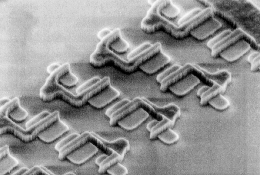
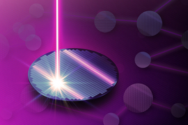
Photolithography uses light to print tiny patterns onto a silicon chip. The patterns are projected over a silicon wafer, which is coated with a chemical that changes its solubility when exposed to light. The soluble parts are etched out, leaving behind tiny structures that become the transistors and other devices on the chip.
Shorter wavelengths of light allow for printing smaller features, enabling more densely packed chips. By the 1980s, the accepted wisdom in the industry was that 248 nm was the shortest wavelength possible for photolithography.
Despite widespread skepticism and technical obstacles, Lincoln Laboratory pioneered photolithography at the 193 nm wavelength, fabricating the world's first microelectronic devices using the technique. The first-ever 193 nm projection system was installed at the laboratory in 1993. Soon after, the laboratory opened its doors to industrial partners to guide 193 nm semiconductor manufacturing and pave the way toward its widespread adoption. Today, it is the industry's mainstream technique and has enabled increasingly powerful integrated circuits.
"Photolithography at 193 nm has enabled the microelectronics industry to continue its path of miniaturization as charted by Moore's law, thus impacting every aspect of our increasingly digital lives. It is also a prime example of the impact that close collaborations between Lincoln Laboratory and industrial partners have had on society," says Mordechai Rothschild, who was one of the key developers of the 193 nm technique and today is a principal staff member in the Advanced Technology Division.
Lighting up a world of new technologies
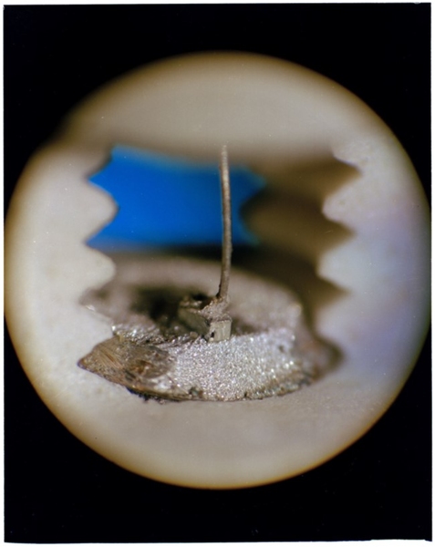
In fall 1962, General Electric, IBM, and Lincoln Laboratory each independently reported the first demonstrations of the semiconductor laser. In the 62 years since, it has become the most widespread laser in the world and a foundational element in a vast range of technologies: DVDs, CDs, computer mice, laser pointers, barcode scanners, medical imagers, and printers, to name a few. However, its greatest impact is arguably in communications. Every second, a semiconductor laser encodes information onto light that is transmitted through fiber-optic cables across oceans and into many homes, forming the backbone of the internet.
While lasers were invented a few years earlier in 1960, the semiconductor type was exceptional because it realized all laser elements — light generation and amplification, lenses, and mirrors — within a piece of semiconducting material no bigger than a grain of rice. When injected with electrical current, the material is extremely efficient at converting the electrical energy to light. These attributes attracted the imagination of scientists and engineers worldwide.
"I'm pretty sure that we wouldn't be streaming movies to our homes or searching for the best restaurants from our phones without the low cost and manufacturability of semiconductor lasers," says Paul Juodawlkis, an expert in photonic devices and integrated circuits, and leader of the laboratory's Quantum Information and Integrated Nanosystems Group. "It's great to know that Lincoln Laboratory has played an important role in advancing this technology for government and commercial applications for the past 60-plus years and is poised to continue doing so in the future."
Honoring inventors and their legacy
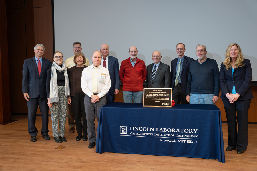
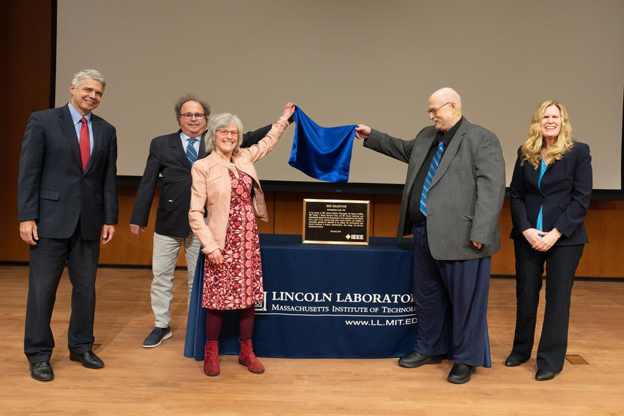
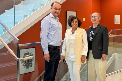
The 2024 IEEE President-elect Kathleen Kramer presented the three awards to Lincoln Laboratory Director Eric Evans during the dedication ceremony. The ceremony was held in the auditorium at Lincoln Laboratory in Lexington, Massachusetts. Evans was joined on stage by inventors or their descendants to receive each plaque. Many Lincoln Laboratory staff and retirees who contributed to these innovations were also in attendance.
Vincent Orlando, who devoted his 50-year career at the laboratory to developing Mode S technology, joined Evans to accept that award. Mordechai Rothschild and David Shaver unveiled the 193 nm photolithography plaque. Both were lead developers of that technology.
For some, the ceremony was a touching celebration of their parent's legacy, and a return to fond memories. Richard Rediker, a son of semiconductor laser inventor Robert Rediker, recalled playing in a lab as a child with his father more than 60 years ago, the last time he visited Lincoln Laboratory. He accepted the semiconductor plaque alongside Susan Zeiger and Robert Lax, children of co-inventors Herbert Zeiger and Benjamin Lax respectively.
"It was so rewarding to meet the other children of my father's colleagues and to fully appreciate what the inventions of our fathers mean to society today. Although my father passed away five years ago, this ceremony brought him back to life for an afternoon," says Rediker, adding that it was an experience he will never forget.
Likewise, these technologies have left an indelible mark on the world.
"By celebrating the pride and prestige of our profession's contributions to history, we demonstrate how engineers, scientists, and technologists have contributed not only to our local communities, but also to our global community," Kramer said, before presenting the plaques. "It is my pleasure to recognize these pioneering events and people behind them. They serve as landmarks in the progress of technology and civilization."
