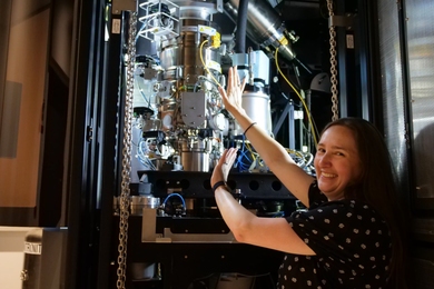
Quantum materials — those with electronic properties that are governed by the principles of quantum mechanics, such as correlation and entanglement — can exhibit exotic behaviors under certain conditions, such as the ability to transmit electricity without resistance, known as superconductivity. However, in order to get the best performance out of these materials, they need to be properly tuned, in the same way that race cars require tuning as well. A team led by Mingda Li, an associate professor in MIT’s Department of Nuclear Science and Engineering (NSE), has demonstrated a new, ultra-precise way to tweak the characteristics of quantum materials, using a particular class of these materials, Weyl semimetals, as an example.
The new technique is not limited to Weyl semimetals. “We can use this method for any inorganic bulk material, and for thin films as well,” maintains NSE postdoc Manasi Mandal, one of two lead authors of an open-access paper — published recently in Applied Physics Reviews — that reported on the group’s findings.
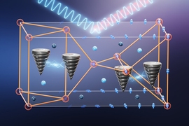
The experiment described in the paper focused on a specific type of Weyl semimetal, a tantalum phosphide (TaP) crystal. Materials can be classified by their electrical properties: metals conduct electricity readily, whereas insulators impede the free flow of electrons. A semimetal lies somewhere in between. It can conduct electricity, but only in a narrow frequency band or channel. Weyl semimetals are part of a wider category of so-called topological materials that have certain distinctive features. For instance, they possess curious electronic structures — kinks or “singularities” called Weyl nodes, which are swirling patterns around a single point (configured in either a clockwise or counterclockwise direction) that resemble hair whorls or, more generally, vortices. The presence of Weyl nodes confers unusual, as well as useful, electrical properties. And a key advantage of topological materials is that their sought-after qualities can be preserved, or “topologically protected,” even when the material is disturbed.
“That’s a nice feature to have,” explains Abhijatmedhi Chotrattanapituk, a PhD student in MIT’s Department of Electrical Engineering and Computer Science and the other lead author of the paper. “When you try to fabricate this kind of material, you don’t have to be exact. You can tolerate some imperfections, some level of uncertainty, and the material will still behave as expected.”
Like water in a dam
The “tuning” that needs to happen relates primarily to the Fermi level, which is the highest energy level occupied by electrons in a given physical system or material. Mandal and Chotrattanapituk suggest the following analogy: Consider a dam that can be filled with varying levels of water. One can raise that level by adding water or lower it by removing water. In the same way, one can adjust the Fermi level of a given material simply by adding or subtracting electrons.
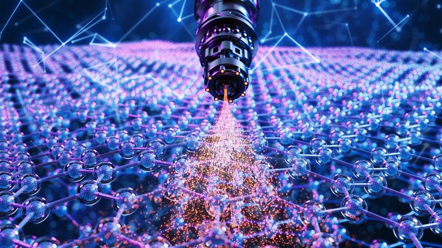
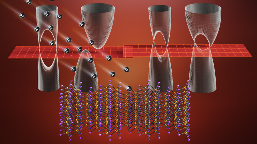
To fine-tune the Fermi level of the Weyl semimetal, Li’s team did something similar, but instead of adding actual electrons, they added negative hydrogen ions (each consisting of a proton and two electrons) to the sample. The process of introducing a foreign particle, or defect, into the TaP crystal — in this case by substituting a hydrogen ion for a tantalum atom — is called doping. And when optimal doping is achieved, the Fermi level will coincide with the energy level of the Weyl nodes. That’s when the material’s desired quantum properties will be most fully realized.
For Weyl semimetals, the Fermi level is especially sensitive to doping. Unless that level is set close to the Weyl nodes, the material’s properties can diverge significantly from the ideal. The reason for this extreme sensitivity owes to the peculiar geometry of the Weyl node. If one were to think of the Fermi level as the water level in a reservoir, the reservoir in a Weyl semimetal is not shaped like a cylinder; it’s shaped like an hourglass, and the Weyl node is located at the narrowest point, or neck, of that hourglass. Adding too much or too little water would miss the neck entirely, just as adding too many or too few electrons to the semimetal would miss the node altogether.
Fire up the hydrogen
To reach the necessary precision, the researchers utilized MIT’s two-stage “Tandem” ion accelerator — located at the Center for Science and Technology with Accelerators and Radiation (CSTAR) — and buffeted the TaP sample with high-energy ions coming out of the powerful (1.7 million volt) accelerator beam. Hydrogen ions were chosen for this purpose because they are the smallest negative ions available and thus alter the material less than a much larger dopant would. “The use of advanced accelerator techniques allows for greater precision than was ever before possible, setting the Fermi level to milli-electron volt [thousandths of an electron volt] accuracy,” says Kevin Woller, the principal research scientist who leads the CSTAR lab. “Additionally, high-energy beams allow for the doping of bulk crystals beyond the limitations of thin films only a few tens of nanometers thick.”
The procedure, in other words, involves bombarding the sample with hydrogen ions until a sufficient number of electrons are taken in to make the Fermi level just right. The question is: how long do you run the accelerator, and how do you know when enough is enough? The point being that you want to tune the material until the Fermi level is neither too low nor too high.
“The longer you run the machine, the higher the Fermi level gets,” Chotrattanapituk says. “The difficulty is that we cannot measure the Fermi level while the sample is in the accelerator chamber.” The normal way to handle that would be to irradiate the sample for a certain amount of time, take it out, measure it, and then put it back in if the Fermi level is not high enough. “That can be practically impossible,” Mandal adds.
To streamline the protocol, the team has devised a theoretical model that first predicts how many electrons are needed to increase the Fermi level to the preferred level and translates that to the number of negative hydrogen ions that must be added to the sample. The model can then tell them how long the sample ought to be kept in the accelerator chamber.
The good news, Chotrattanapituk says, is that their simple model agrees within a factor of 2 with trusted conventional models that are much more computationally intensive and may require access to a supercomputer. The group’s main contributions are two-fold, he notes: offering a new, accelerator-based technique for precision doping and providing a theoretical model that can guide the experiment, telling researchers how much hydrogen should be added to the sample depending on the energy of the ion beam, the exposure time, and the size and thickness of the sample.
Fine things to come with fine-tuning
This could pave the way to a major practical advance, Mandal notes, because their approach can potentially bring the Fermi level of a sample to the requisite value in a matter of minutes — a task that, by conventional methods, has sometimes taken weeks without ever reaching the required degree of milli-eV precision.
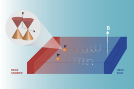
Li believes that an accurate and convenient method for fine-tuning the Fermi level could have broad applicability. “When it comes to quantum materials, the Fermi level is practically everything,” he says. “Many of the effects and behaviors that we seek only manifest themselves when the Fermi level is at the right location.” With a well-adjusted Fermi level, for example, one could raise the critical temperature at which materials become superconducting. Thermoelectric materials, which convert temperature differences into an electrical voltage, similarly become more efficient when the Fermi level is set just right. Precision tuning might also play a helpful role in quantum computing.
Thomas Zac Ward, a senior scientist at the Oak Ridge National Laboratory, offered a bullish assessment: “This work provides a new route for the experimental exploration of the critical, yet still poorly understand, behaviors of emerging materials. The ability to precisely control the Fermi level of a topological material is an important milestone that can help bring new quantum information and microelectronics device architectures to fruition.”
